Thank you for your participation in this survey. A gift card will be sent to the email address you have provided.
We are here to help you with your most challenging production, R&D, and engineering issues.
Physical Electronics (PHI), the premier name in surface analysis offers analytical services using our state-of-the-art instruments. Our scientists have a deep knowledge of surface analysis applications and problem solving, and the benefit of always having access to the latest instrument technology. It is a winning combination to help you tackle your most challenging production, R&D, and engineering issues.
To discuss a particular project or to request a quote, please contact PHI at analysis@phi.com or 952-828-6426
Common Applications
|
|
- Materials properties engineering and validation
- Surface defects and contamination
- Failure analysis and process control
- Coatings and interfaces
- Thickness and composition
- Nanomaterials and thin films structural characterization
- Metrological application
- Competitive analysis
|
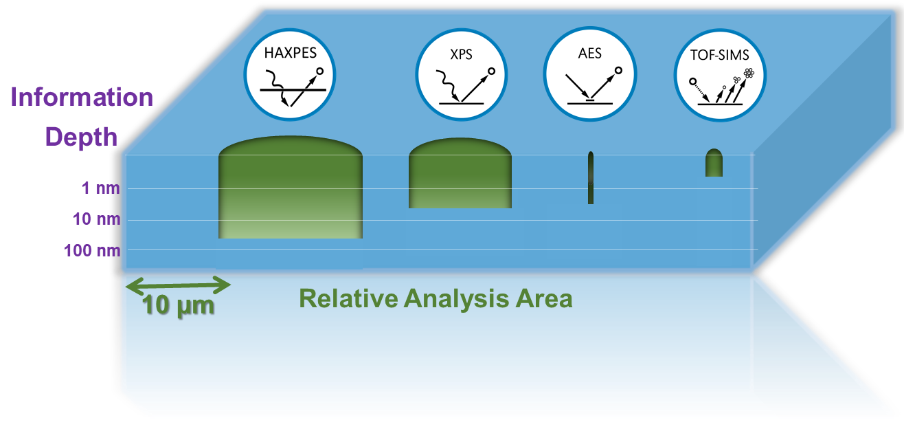 |
XPS - X-Ray Photoelectron Spectroscopy
- PHI Quantera and VersaProbe III scanning XPS microprobe systems with spectroscopic spatial resolution <10um
- Quantification and chemical state analysis
- Multiple ion beams available for optimized depth profiling of organics, inorganics and mixed materials
- Angle-dependent analysis for thin film characterization
- Inert gas sample transfer for air sensitive samples
- Electronic band structure analysis
- In-situ heating and cooling
- In-situ sample biasing experiments
- Also available: C60 ion and argon gas cluster ion (GCIB) sputter depth profiling
|
 |
|
|
HAXPES - Hard X-Ray Photoelectron Spectroscopy
- PHI Quantes scanning XPS/HAXPES microprobe system with Spectroscopic spatial resolution < 14 µm
- Quantification and chemical state analysis from 3 times the depth of XPS for probing thicker film structures and buried interfaces
- Same are XPS and HAXPES analysis
- Multiple ion beams available for optimized depth profiling of both organic and inorganic materials
- Inert gas sample transfers for air sensitive samples
|
 |
|
|
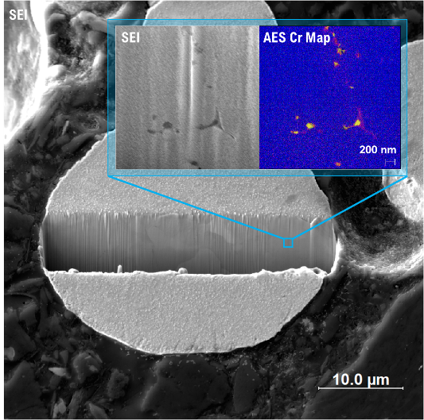
AES - Auger Electron Spectroscopy
- PHI 710 field emission Auger system with analytical spatial resolution < 8 nm
- Surface sensitive compositional analysis
- Ion sputter depth profiling
- In-situ sample fracturing
- In-situ cryogenic sample fracturing
- Focused Ion Beam (FIB)
- Energy Dispersive X-ray Spectroscopy (EDS)
|
 |
|
|
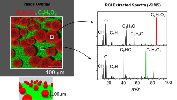
TOF-SIMS - Time-of-Flight Secondary Ion Mass Spectrometry
- PHI nanoTOF II TOF-SIMS Analysis with <70 nm spatial resolution
- Surface sensitive molecular imaging and trace analysis
- Multiple ion beams available for optimized depth profiling of organics, inorganics and mixed materials
- In-situ Focused Ion Beam (FIB) cross-sectioning
- Tandem mass (MS/MS) analysis for unambiguous peak identification
- In-situ sample heating and cooling
|
 |
|
|
All techniques also offer the option of inert gas transfer of samples from a dry glove box to the instruments without exposure to air.
To discuss a particular project or to request a quote, please contact PHI at analysis@phi.com or 952-828-6426
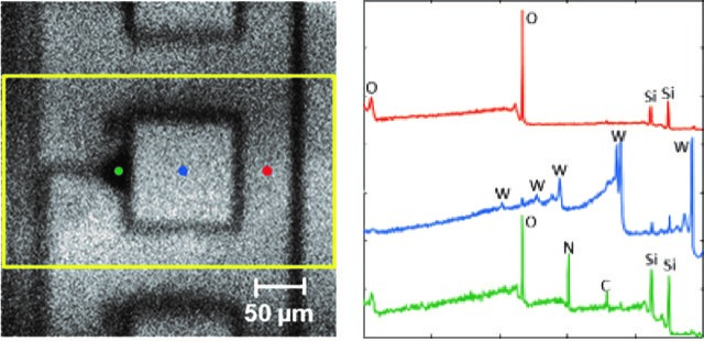
"PHI was an extremely valuable resource for our investigations into a major issue in some of our products. PHI's TOF-SIMS studies helped us nail down exactly which film was compromised. Armed with that information, we managed to successfully address the problem, and PHI was a significant contributor to that success."
- Semiconductor Contract Customer -