Physical Electronics (PHI), the premier name in surface analysis offers analytical services using our state-of-the-art instruments. Our scientists have a deep knowledge of surface analysis applications and problem solving, and the benefit of always having access to the latest instrument technology. It is a winning combination to help you tackle your most challenging production, R&D, and engineering issues.
To discuss a particular project or to request a quote, please contact PHI at analysis@phi.com or call us at 518-650-1892 8 a.m.-5 p.m. CST
Common Applications
|
|
- Materials properties engineering and validation
- Surface defects and contamination
- Failure analysis and process control
- Coatings and interfaces
- Thickness and composition
- Nanomaterials and thin films structural characterization
- Metrological application
- Competitive analysis
|
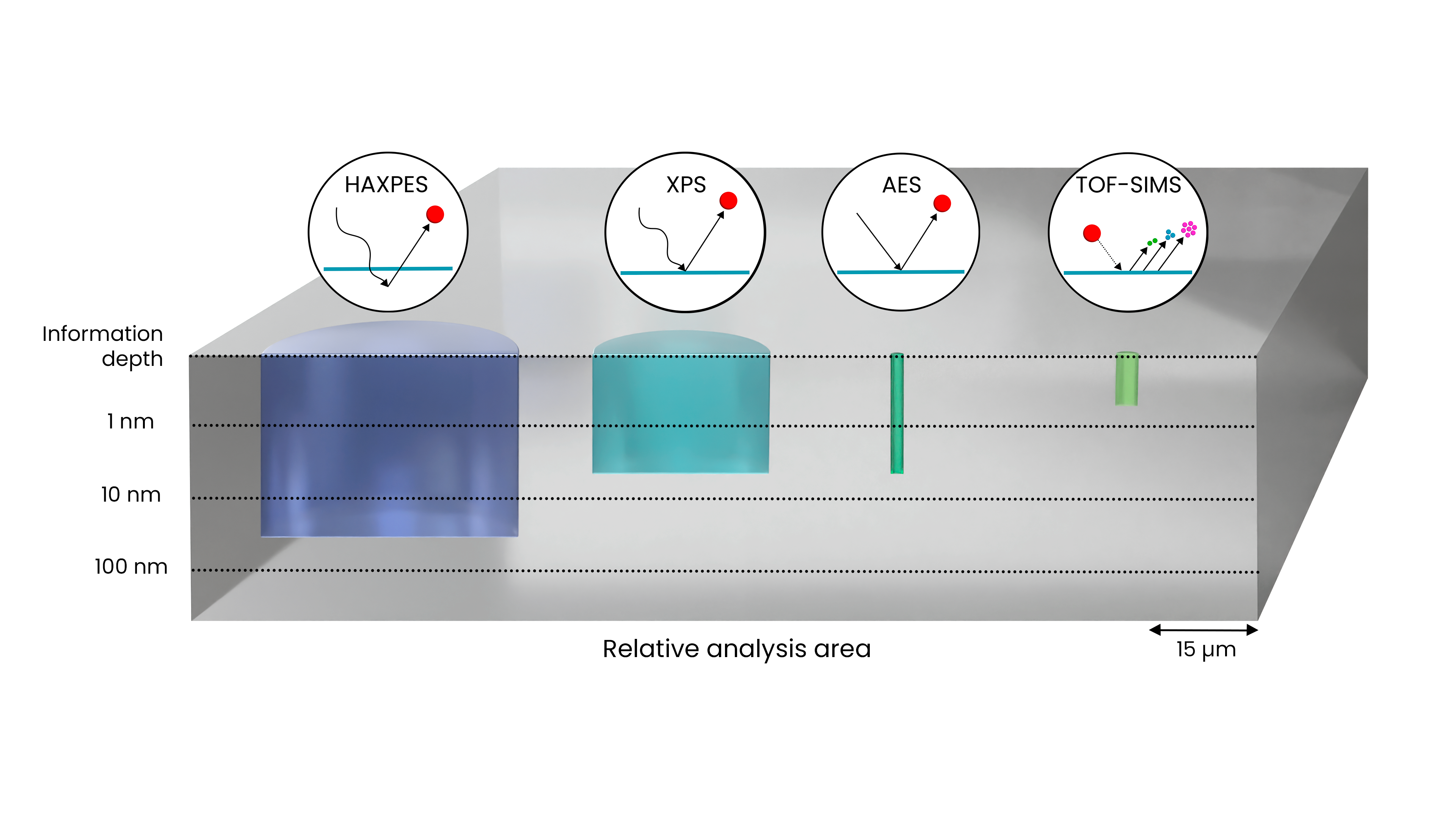 |
XPS - X-Ray Photoelectron Spectroscopy
- Quantitative elemental and chemical-state spectroscopy up to 10 nm below a material’s surface, which allows for probing film structures and buried interfaces
- Angle-resolved analysis for non-destructive multi-layer film thickness measurements (AR-XPS)
- Inert sample transfer vessel for air-sensitive samples
- Monoatomic argon (Ar+) and argon gas cluster ion beam (GCIB) for optimized sputter depth-profiling of organics, inorganics, and mixed materials
- XPS analysis is performed on the PHI Quantes Scanning XPS/HAXPES Microprobe instrument with Al Kα X-ray source
|
 |
|
|
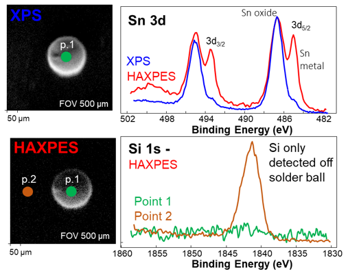
HAXPES - Hard X-Ray Photoelectron Spectroscopy
- Quantitative elemental and chemical-state spectroscopy up to 30 nm below a material’s surface, which allows for probing thicker film structures and buried interfaces
- HAXPES is a complementary technique available on the same instrument as XPS, allowing for analysis of the same region of interest on the sample surface
- Angle-resolved analysis for non-destructive multi-layer film thickness measurements (AR-HAXPES)
- Inert sample transfer vessel for air-sensitive samples
- Monoatomic argon (Ar+) and argon gas cluster ion beam (GCIB) for optimized sputter depth-profiling of organics, inorganics, and mixed materials
- HAXPES analysis is performed on the PHI Quantes Scanning XPS/HAXPES Microprobe instrument with Cr Kα X-ray source
|
 |
|
|
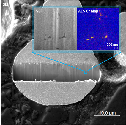
AES - Auger Electron Spectroscopy
- Quantitative elemental spectroscopy and nanoscale surface imaging up to 10 nm below a material’s surface, which allows for probing film structures and buried interfaces
- SEM-like (scanning electron microscopy) imaging with spatial resolution < 8 nm
- AES is the nanoscale counterpart of the traditional SEM-EDS (energy dispersive X-ray spectroscopy) technique
- Inert sample transfer vessel for air-sensitive samples
- Monoatomic argon (Ar+) sputter depth-profiling
- AES analysis is performed on the PHI 710 Multi-Technique Scanning Auger Nanoprobe
|
 |
|
|
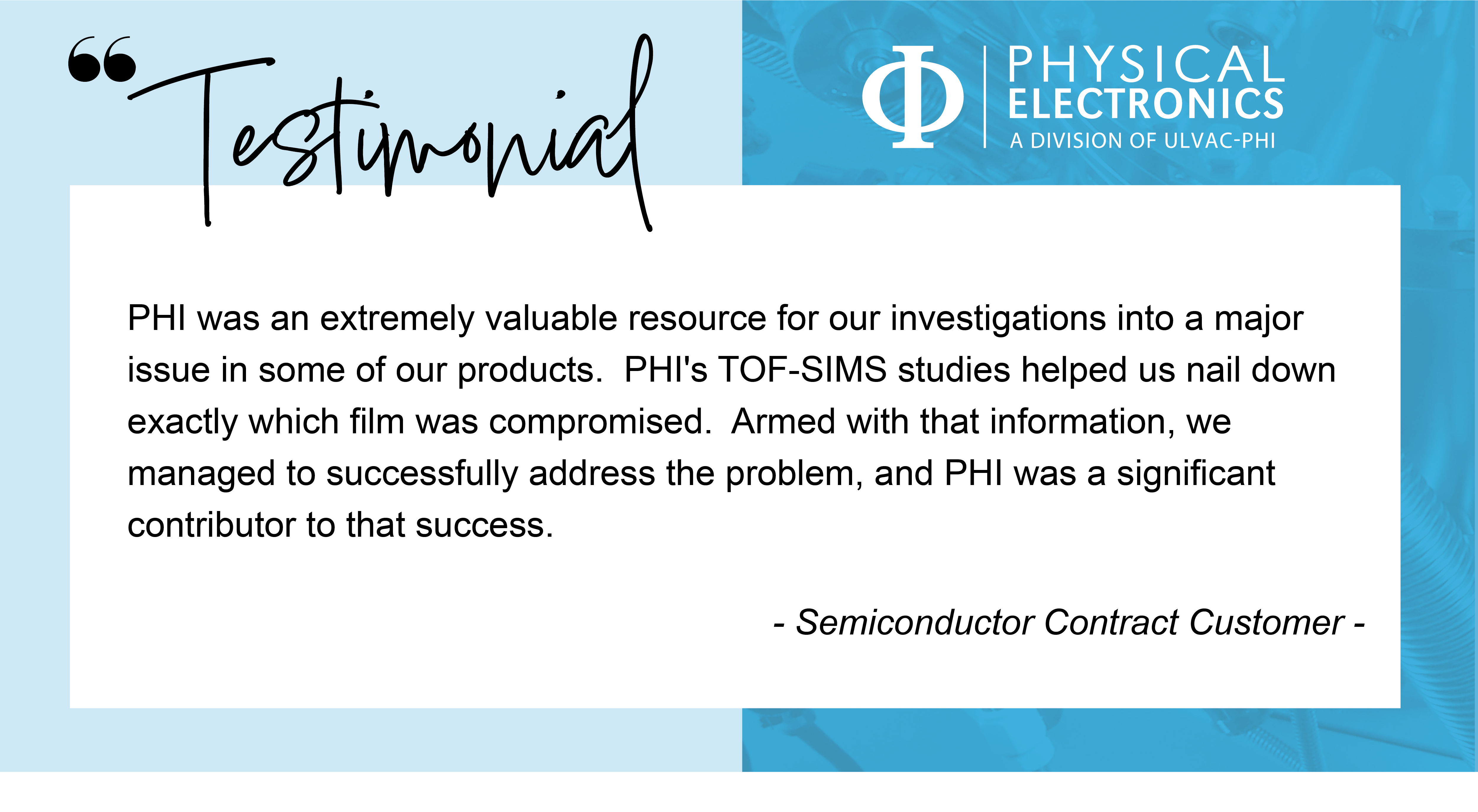
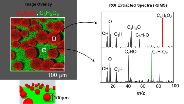
TOF-SIMS - Time-of-Flight Secondary Ion Mass Spectrometry
- Surface mass spectrometry, elemental & molecular imaging, and trace analysis
- Spatial resolution < 70 nm with 1-2 nm sampling depth below a material’s surface
- Detection limit of parts per million (PPM) and parts per billion (PPB)
- Inert sample transfer vessel for air-sensitive samples
- Multiple ion beams available for optimized sputter depth-profiling of organics, inorganics, and mixed materials: cesium (Cs+), oxygen (O2+), monoatomic argon (Ar+), gas cluster ion beam (GCIB)
- Tandem mass spectrometry (MS/MS or MS2) for unambiguous peak identification
- TOF-SIMS analysis is performed on the PHI nanoTOF II instrument
|
 |
|
|
To discuss a particular project or to request a quote, please contact PHI at analysis@phi.com or call us at 518-650-1892 8 a.m.-5 p.m. CST.